Voltage Doubler


Theory

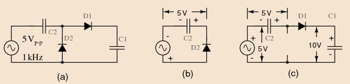
The half-wave voltage doubler shown in figure below (a) is composed of two circuits: a clamper at (b) and peak detector (half-wave rectifier) in Figure prior, which is shown in modified form in (c). C2 has been added toa peak detector (half-wave rectifier).


Fig.1 Diagram of Voltage Doubler

Referring to Figure above (b), C2 charges to 5 V (4.3 V considering the diode drop) on the negative half cycle of AC input. The right end is grounded by the conducting D2. The left end is charged at the negative peak of the ACinput. This is the operation of the clamper.

During the positive half cycle, the half-wave rectifier comes into play at Figure above (c). Diode D2 is out of the circuit since it is reverse biased. C2 is now in series with the voltage source. Note the polarities of the generator and C2, series aiding. Thus, rectifier D1 sees a total of 10 V at the peak of the sinewave, 5 V from generator and 5 V from C2. D1 conducts waveform v (1) (Figure below), charging C1 to the peak of the sine wave riding on 5 V DC (Figure below v (2)). Waveform v (2) is the output of the doubler, which stabilizes at 10 V (8.6 V with diode drops) after a few cycles of sinewave input.