 |
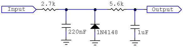
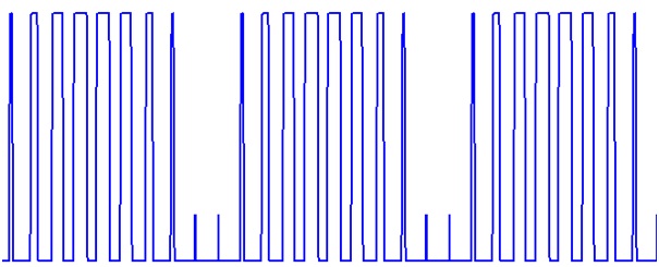
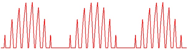
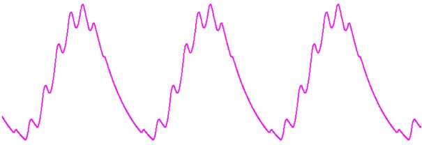
The PWM signal shown in figure: 1 is applied to an integrator and hold circuit. When the positive edge of pulse appears, the integrator generates ramp output whose magnitude is proportional to the pulse width. After the negative edge, the hold circuit maintains the peak ramp voltage for a given period and then forces the output voltage to zero. The waveform is the sum of Vb and a sequence of constant-amplitude and constant-width pulse generated by demodulator. This signal is then applied to the input of clipping circuit, which cuts off the portion of signal below the threshold voltage Vth and outputs the reminder. Therefore the output of clipping circuit is a PAM signal whose amplitude is proportional to the width of PWM signal, Finally, the PAM signal passes through a simple low-pass filter and the original audio signal is obtained.
 |
 |
 |