 |
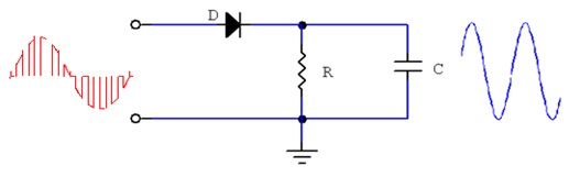
In this circuit diode D is the detector diode, the resistance R is the load resistance and C is the filter capacitor. In the positive half cycle of PAM signal, diode conducts and current flows through R, whereas in negative half cycle, the diode is reversed biased and no current flows. Therefore only positive half of the PAM wave appears across resistance R. the capacitor across R provide low impedance at the carrier frequency and much higher impedance at the modulating frequency. Therefore capacitor reconstructs the original modulating signal.
The circuit relies upon the behavior of the diode allowing current through when the input is positive with respect to the capacitor voltage, hence topping up the capacitor voltage to the peak level, but blocking any current from flowing back out the diode when the input is below the capacitor through the current they pass varies the applied voltage, as a result the modulated output is slightly distorted in a way which depends upon the diodes I / V characteristics. The circuit also suffers from the problem known as ripple and negative peak Clipping. The ripple effect happens because the capacitor will be discharged a small amount in between successive peaks of the input PAM wave.
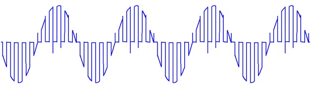 |
The modulated waveform or signal which wants to demodulate is as above, this signal is provided to the demodulator circuit to recover the signal from it. In the positive half cycle of PAM signal, diode conducts and current flows through R, whereas in negative half cycle, the diode is reversed biased and no current flows. After providing the signal to demodulator circuit, the Detector diode works as a half wave rectifier and rectify the positive half waves and fed it to RC filter.
 |