 |
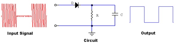
In this circuit diode D is the detector diode, the resistance R is the load resistance and C is the filter capacitor. In the positive half cycle of ASK signal, diode conducts and current flows through R, whereas in negative half cycle, the diode is reversed biased and no current flows. Therefore only positive half of the ASK wave appears across resistance R. the capacitor across R provide low impedance at the carrier frequency and much higher impedance at the modulating frequency. Therefore capacitor reconstructs the original modulating signal.
The circuit relies upon the behavior of the diode allowing current through when the input is positive with respect to the capacitor voltage, hence topping up the capacitor voltage to the peak level, but blocking any current from flowing back out the diode when the input is below the capacitor through the current they pass varies the applied voltage, as a result the modulated output is slightly distorted in a way which depends upon the diodes I / V characteristics. The circuit also suffers from the problem known as ripple and negative peak Clipping. The ripple effect happens because the capacitor will be discharged a small amount in between successive peaks of the input ASK wave.
The R - C coupling is work like as low pass filter, it remove the high frequency components, and the remains part of the input waveform is original signal which sent for conveying the information by amplitude modulation.
The output of this circuit is a signal which sent to conveying the message by Amplitude Shift Keying. The amplitude and frequency of this recovery signal should be same as that signal which provided for modulation.